Jump to content

File:Illustration of C-V measurement.gif

Illustration_of_C-V_measurement.gif (322 × 308 pixels, file size: 93 KB, MIME type: image/gif, looped, 18 frames, 5.4 s)

Summary

Description
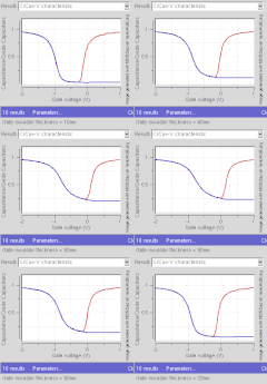
English: C-V measurements can reveal oxide thickness, oxide charges, contamination from mobile ions, and interface trap density in wafer processes. In this image the C-V profile for a bulk p-type substrate MOSCAP with different oxide thickness is shown. The blue curve shown refers to a high frequency C-V profile while the red curve refers to low frequency C-V profile. MOS capacitance is independent of all the frequencies in the accumulation and depletion region. This is because it is here that the total charge is governed by majority carriers. In the inversion region the charge is governed by minority carriers, which forms the inversion layer. Due to finite minority carrier generation time, total charge is not able to follow the gate bias at higher frequencies, which can lead to differences in C-V profiles. Also worth noting here is the shift in threshold voltage with different oxide thickness.
Date
Source Image:https://nanohub.org/resources/8818 ; Tool link: http://nanohub.org/resources/451
Author Saumitra R Mehrotra & Gerhard Klimeck
Permission
(Reusing this file)

Licensing

w:en:Creative Commons
attribution
This file is licensed under the Creative Commons Attribution 3.0 Unported license.
Attribution: Saumitra R Mehrotra & Gerhard Klimeck
You are free:
  • to share – to copy, distribute and transmit the work
  • to remix – to adapt the work
Under the following conditions:
  • attribution – You must give appropriate credit, provide a link to the license, and indicate if changes were made. You may do so in any reasonable manner, but not in any way that suggests the licensor endorses you or your use.

Captions

Add a one-line explanation of what this file represents

Items portrayed in this file

depicts

3 February 2010

95,693 byte

5.4 second

308 pixel

322 pixel

image/gif

829e4f95f22a9809858077490f51655c5197ada3

File history

Click on a date/time to view the file as it appeared at that time.

Date/TimeThumbnailDimensionsUserComment
current19:26, 17 May 2010Thumbnail for version as of 19:26, 17 May 2010322 × 308 (93 KB)Beatnik8983{{Information |Description={{en|1=C-V measurements can reveal oxide thickness, oxide charges, contamination from mobile ions, and interface trap density in wafer processes. In this image the C-V profile for a bulk p-type substrate MOSCAP with different ox

The following 2 pages use this file:

Global file usage

The following other wikis use this file:

See what we do next...

OR

By submitting your email or phone number, you're giving mschf permission to send you email and/or recurring marketing texts. Data rates may apply. Text stop to cancel, help for help.

Success: You're subscribed now !